FPGA Infrastructure
Hardware Overview
The Noctua 2 FPGA infrastructure consists of 36 nodes in the fpga partition and 3 heterogeneous accelerator nodes in the hacc partition. Note that not only the dedicated hacc-nodes, but all nodes with AMD/Xilinx FPGAs are accessible as part of the Heterogeneous Accelerated Compute Clusters (HACC) program via a small project proposal for FPGA researchers worldwide.
A technical description of Noctua 2 and the FPGA partition can be found in the Noctua 2 paper.
| Xilinx Alveo U280 Nodes | Intel Stratix 10 Nodes | Custom Configuration Nodes | HACC Nodes |
|---|---|---|---|---|
Number of Nodes | 16 | 16 | 4 | 3 |
| ||||
Accelerator Cards | 3x Xilinx Alveo U280 cards | 2x Bittware 520N cards |
| 2x Xilinx Alveo U55C cards |
FPGA Types | Xilinx UltraScale+ FPGA (XCU280, 3 SLRs) | Intel Stratix 10 GX 2800 FPGA | Xilinx UltraScale+ FPGA (3 SLRs) | |
Main Memory per Card | 32 GiB DDR | 32 GiB DDR | - | |
High-Bandwidth Memory per Card | 8 GiB HBM2 |
| 8 GiB HBM2 | |
Network Interfaces per Card | 2x QSFP28 (100G) links | 4x QSFP+ (40G) serial point-to-point links | 2x QSFP28 (100G) links (U55C) | |
Topology of System | ||||
| ||||
CPUs | 2x AMD Milan 7713, 2.0 GHz, each with 64 cores | 2x AMD Milan 7V13, 2.45 GHz, each with 64 cores | ||
Main Memory | 512 GiB | 512 GiB | ||
Storage | 480 GB local SSD in | full access to the Noctua 2 shared file systems | ||
|
| |||
Application-specific interconnect | Connected via CALIENT S320 Optical Circuit Switch (OCS), configurable point-to-point connections to any other FPGA or to a 100G Ethernet switch, more details see FPGA-to-FPGA Networking. | |||
The software environment is setup using modules, see section Software Overview. For hardware execution, FPGA nodes with the correct configuration and driver version (so-called board support package or BSP) need to be allocated, see section FPGA System Access to FPGA Partition.
Software Overview
The software environment is setup using modules. Depending on the user requirements, different development flows for the FPGA cards are supported.
Xilinx Alveo U280
Vitis Design Flow (recommended)
Vivado Design Flow
Intel Stratix 10
oneAPI (recommended)
OpenCL (recommended for projects with exisiting OpenCL code base or for usage of serial channels)
DSP Builder
The development (including emulation to check functional correctness, report generation to get indications of expected performance, and synthesis with bittstream generation) can be done on any Noctua 2 node. Just load the corresponding modules for the target FPGA platform and Development Tool flow.
To execute designs on actual FPGAs, the same modules are required and additionally an FPGA node needs to be allocated with a fitting constraint, to get FPGAs with the expected configuration and drivers.
The Table of FPGA Software and Firmware Stacks provides an overview of the interplay of tools, modules and constraints for the three recommended development flows. Additionally, we have created Quick Start Guides to walk you through the six steps with examples using the latest tools.
System Access to FPGA Partition
To use Noctua 2 nodes with FPGAs, along with your Slurm command, you need to select the FPGA partition and provide a constraint to specify the configuration of FPGAs (shell, driver, board support package (BSP)) that your designs have been built for.
For Xilinx Alveo U280 cards you can use
srun --partition=fpga --constraint=xilinx_u280_xrt2.12 -A [YOUR_PROJECT_ACCOUNT] -t 2:00:00 --pty bash
For Bittware 520n cards with Intel Stratix 10 FPGAs you can use
srun --partition=fpga --constraint=bittware_520n_20.4.0_max -A [YOUR_PROJECT_ACCOUNT] -t 2:00:00 --pty bash
Constraints can be used together with srun, sbatch and salloc, however under some conditions salloc will fail, for details click the expansion box below. We recommend to always use srun or sbatch.
A list of available matching versions of the BSPs and SDKs can be found in the Software Overview Details.
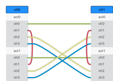
Serial Channels between FPGAs
When configured with a correct BSP, all FPGA boards offer 4 point-to-point connections to other FPGA boards. FPGA Serial Channels have an own documentation page with various examples and a graphical input tool (see figure below).
Sanity Checks and Troubleshooting
Tool and Board Info
Hardware Diagnose
link to main sanity checks and troubleshooting page
Contact and Support
For problems with the FPGA infrastructure (software and/or hardware) use our main support mail address pc2-support@uni-paderborn.de.
In order to help you as quickly as possible, please follow these guidelines
Use
[Noctua2-FPGA]as a prefix in your email subject line.Where did the problem occur and what did you expect to happen?
If possible, how can we reproduce the error in a systematic manner?
Did you attempt to fix/troubleshoot the problem? If you attempted to debug the problem, provide us the steps you already took and the intermediate results.
For general questions, acceleration support or project ideas with regarding FPGAs, please reach out to the FPGA domain-expects.
Getting Started
As a beginner with FPGAs it might take a lot of time to learn about the different concepts to setup the environment, compile code and actually run it on an FPGA. The good news is, that most of the knowledge can be boiled down to 6 steps that are very similar for the different development flows. We have created Quick Start Guides to walk you walk you through the six steps with examples using the latest tools.
The general structure of the quick start guides is the following:
1. Get Example Code
All development flows are shipped with design examples. In this step you learn how to get the code and the structure of the examples.
2. Setup the Environment
All development flows are loaded with modules. In this step you learn which modules are required to establish a working environment.
3. Build and Execute in Emulation
Build and execute in emulation: Most of the FPGA code development will be done in emulation (run the code on CPU), because the actual FPGA code generation is very time consuming. In this step you learn how to build and run the code in emulation.
4. Create and Inspect Reports
Reports can be generated quickly during code compilation. It is crucial for any efficient FPGA development process to analyze reports regularly prior to actual hardware builds. In this step you learn how to generate the reports and which indicators are good starting point to estimate the efficiency on an actual FPGA.
5. Build the Hardware Design
The hardware build step (so-called hardware synthesis) can take lots of time and compute resources. In this step you learn how to create batch scripts to submit the synthesis job to the slurm workload manager.
6. Execute Design on FPGA Hardware
After the hardware synthesis, we can allocate an FPGA node for execution. In this step you learn how to allocate a correctly configured FPGA node that matches the soft- and hardware requirements.
Available FPGA Libraries and Applications
We and others have developed several ready to use libraries and applications that use FPGAs to accelerate the computation. Please use the links to get examples and the documentation. You can contact us, if you need guidance to accelerate your target code with our FPGAs libraries.
Application | Toolchain | Type of Support |
|---|---|---|
OpenCL | Ready-to-use module files and bitstreams deployed on Noctua 2 | |
OpenCL | FPGA support in CP2K main repository + extra repository with FPGA designs fitting the Bittware 520N cards in Noctua 2 | |
OpenCL | Repository with benchmark suite targeting FPGAs from Intel (including the Bittware 520N with Stratix 10 cards in Noctua 2) and Xilinx | |
OpenCL | Repository with implementation of Cannon matrix multiplication as building block for GEMM on FPGAs fitting the Bittware 520N cards in Noctua 2 | |
Repository with library and examples build with oneAPI for stencil simulations on FPGAs fitting the Bittware 520N cards in Noctua 2 |
Related pages